


.png)
Introduction
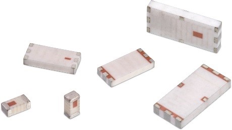
The trend to miniaturize wireless communication devices has led to decreased PCB sizes and increased component densities. Although this shift to miniaturized technology has aided many areas of electronic design, it constrains RF front-end design. Due to the nature of antennas sending and receiving electromagnetic signals, they interact and are affected by the entire surrounding environment and are extremely sensitive to electromagnetic fields. This can be extremely problematic for RF engineers when integrating into a design an antenna that is small, has good gain and efficiency in the frequency range of operation, and is able to work as desired in different PCB environments. Multilayer chip antennas are an interesting choice for engineers, who are restricted by cost and space requirements in wireless system design. Low temperature co-fired ceramic (LTCC) multilayer chip antennas are formed from several layers of dielectric material, which are pressed and fired together into a monolithic structure. Each dielectric layer has patterned metallization on the surface that connects to other layers through vias. The layers and vias form a helical multilayer antenna. This application note explains how to get the maximum performance from the Würth Elektronik WE-MCA Multilayer Chip Antenna with respect to antenna placement on a PCB and effective impedance matching.
2 Antenna design and simulation
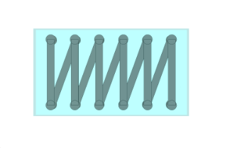
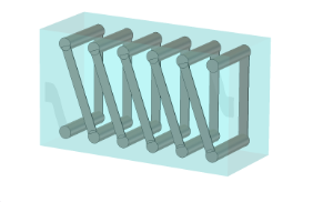
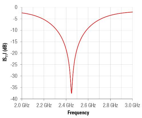
The importance of antenna placement is clearly understandable when the structure and operating principle of an antenna are considered. For this purpose, the WE-MCA Multilayer Chip Antenna (748 893 02 45) has been simulated in a 3D electromagnetic design tool (CST Microwave studio, CST, Germany) to illustrate electromagnetic fields and radiation patterns. The multilayer chip antenna consists of metallic layers, connected by vias and enclosed by ceramic material (Figure 2). The inner conductors and vias form the radiating, multilayer meander structure. Electromagnetic fields are generated by the currents on the inner conductor (Figure 3). This self-resonating meander structure allows the component to be smaller than a monopole antenna while achieving comparable performance. The antenna is designed to operate at a centre frequency of 2.45 GHz (Bluetooth/Wi-Fi) with a 10 dB bandwidth of more than 250 MHz with more than 30 dB return loss as evidenced by the simulated S-parameters (Figure 4).

3 Antenna PCB placement considerations
When incorporating an antenna into an electrical product, some of the most critical stages of product development are the design of PCB layout and device enclosures. This is due to PCB component density continuously being increased to reduce the size of the device while not impairing the function of the design. Antennas can be extremely sensitive to power and ground planes when functioning as a λ/4 monopole antenna system. However, if the feedline and ground plane dimensions are carefully and intelligently taken into consideration when designing a chip antenna PCB, performance comparable to a λ/2 dipole antenna can be achieved. The positioning of the WE-MCA is critical to achieving optimum antenna gain and performance. The antenna gain can be significantly reduced when the design rules are not followed. Generally, the closer a grounded conductive material is placed to the antenna, the lower the performance will be.
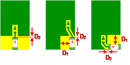
3.1. Corner placement
Placing the antenna on the PCB corner is generally the most desirable location. This typically results in better antenna gain. If the antenna is placed in a corner, it will be surrounded by a ground plane on only two sides. When the antenna is placed in the corner of a PCB, the following criteria should be implemented to achieve optimum antenna performance (Figure 5).
3.2. Side placement
The antenna may be placed on the side of the PCB where it is surrounded on three sides by ground plane when it is not possible to place the antenna on the corner, although antenna performance may be reduced. To ensure the best performance in this position, the following design criteria need to be met (Figure 6).
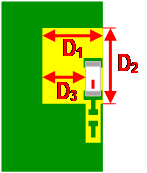
3.3. Ground placement
In extreme cases, the antenna may be placed over or between ground planes. However, it must be remembered that having any metal plate or battery, above or below the antenna will also result in significant degradation of antenna performance. In some cases, there is no other alternative except to utilize the area above or below the antenna and so careful consideration must be taken during the design and prototype stages to ensure sufficient antenna gain performance. In this case, the ground planes must be a minimum of 6 mm above or below the antenna area
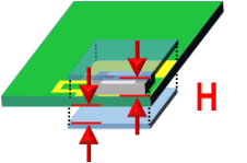
3.4. Device enclosures
Special considerations should be taken into account when an antenna is placed in an enclosure. Completely encasing the antenna in metallic casing/housing/enclosure is out of question, since the majority of the power from the antenna will be reflected back into the device. Housing made of non-conductive materials, such as plastic and glass, are much easy to incorporate into a design than conductive materials. Although the power is not reflected, the impedance and overall performance of the antenna will be effected. Depending on the non-conductive material permittivity and proximity to the antenna, a significant frequency shift of up to hundreds of MHz can be expected. This needs correcting with appropriate impedance matching.
4 Impedance matching
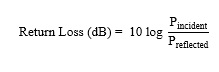
Usually when a chip antenna is designed, the electrical specifications are measured on a manufacturer’s test board, in free space. In reality, an antenna will be operated in an environment that results in an impedance transformation, regardless of whether it is intended or not, with the impedance mismatch being different for every device. Antenna return loss is a good measure of how well an antenna is matched to its feed line. Return loss quantifies the amount of power being reflected by the antenna mismatch back to the source (Equation 1). In an ideal world, a perfectly matched antenna would transmit 100 % of the incident power with 0 % return loss. Since no components are ideal, there are always undesired losses. A return loss of 10 dB is acceptable, and means 90 % power transfer while a return loss of 20 dB is equivalent to 99 % power transfer.
Impedance matching is carried out to mitigate mismatches caused by board placement, the surrounding components and enclosure and the presence or absence of overlapping ground planes. This requires the addition of capacitance or inductance to an antenna circuit to ensure the voltage and current are in-phase. This minimizes the amount of reflected power and reduces VSWR (voltage standing wave ratio) meaning efficient power transfer to and from the antenna, therefore the maximum power is being transferred to and from the antenna by the feedline.
In the design and development of a product, special space needs to be allocated for a matching network during PCB design for RF inductors and/or capacitors, the values of which need to be determined and optimized during the prototyping stage. Matching networks are implemented as close to the load or source as possible, as the length of feedline will have an effect on the impedance matching and power transfer. At microwave frequencies, the input impedance changes with respect to distance from source, unless the transmission line is matched to the load/source with the characteristic impedance.
The impedance can be measured with the help of Vector Network Analyzers (VNAs). VNAs are able to measure the amplitude and phase angle of a system. The measurements can be displayed in a number of formats but S-parameters and the Smith Chart are the most useful tools when matching the impedance of an antenna.
4.1. S-parameters
S-parameters are part of a larger group of similar parameters (e.g. Z-parameters, Y-parameters) and use matched loads to characterize a system. For S-parameters, the system containing any number and variety of components is treated as a black box with ports. S11 provides information about the amount of power that is being reflected (return loss) back to the port while S21 is the power that is being transmitted (insertion
loss) from port 1 to port 2. Measurements are represented as a complex number that corresponds to magnitude and phase angle. This can be displayed in either Cartesian form, where magnitude and phase are presented in decibels and degrees, or polar form, where a data point represents a measurement at one frequency or a locus for a data spectrum.
4.2. Smith Charts
The Smith Chart is a graphical tool that plots the complex impedances in polar form and is commonly used by RF engineers to facilitate transmission line theory problems. The true power of the Smith Chart lies in its ability to display multiple parameters of interest simultaneously. Some of these parameters include impedance, admittance, S-parameters, VSWR and constant gain circles. Looking at Figure 8, the collection of circles, arcs and lines can initially seem quite intimidating. However, in reality, only a few simple things need to be understood to correctly interpret it. The red circles and red arcs that we see in Figure 8 are resistance and reactance lines respectively and are always touching the chart outline at 90°. It must be remembered that the resistance and reactance remain constant if the movement is along these circles and arcs. Similarly, the blue circles and curves that are touching the outline of the Smith Chart at 270 ° are called conductance and susceptance lines. At the center of the Smith Chart is the 50 Ω point, which is also the point of interest since the characteristic impedance (Z0) of antennas is almost always 50 Ω.
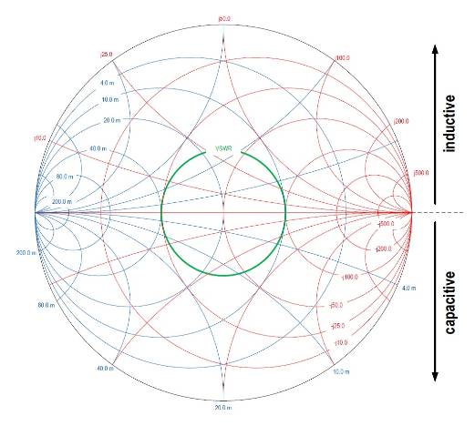
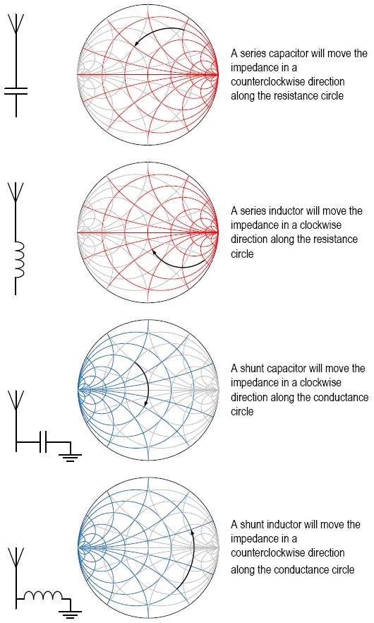
Once a measurement is made, it appears on the Smith Chart as a complex impedance with resistive and reactive components. The goal in this case is to move the impedance at the antenna operating frequency to the center of the Smith Chart (50 Ω). This can be achieved using RF inductors and/or capacitors. A pi-network is especially useful for this purpose as it can be used in a very flexible way for antenna tuning to 50 Ω from almost any other value. In typical scenarios, only two reactive components (inductor and capacitor) are needed to match the impedance to 50 Ω, but a pi network should always be implemented in PCB design to offer maximum flexibility later in the development process. Using the principles below, it can be visualized what components need to be used and in which topology to achieve the desired matching.
5 WE-MCA matching example
Now we know the design rules needed to achieve the best performance characteristics from the WE-MCA, an example of the matching process will be demonstrated. This was done on a demonstration board with the RF inductors coming from the WE-MK Multilayer Ceramic SMD Inductor Design Kit (744 784 A) available to customers with free refills and a Keysight E5071C vector network analyzer (Santa Rosa, USA).
Before calibration, set the VNA to a frequency range that covers the entire band of interest and a little more. For example, the WE-MCA (748 891 02 45) covers a frequency range of 2.4 to 2.5 GHz so the VNA was set to 2 to 3 GHz. It is important to correctly calibrate the VNA according to the manufacturer specifications to negate the phase shift caused by the connecting cable. Without correct calibration, achieving a matched antenna will still be possible but it will be much harder to interpret the Smith Chart data. To check the quality of the calibration, a short, open and load can be connected to the cable and the measurements viewed on the Smith Chart. The trace should appear on the left (short), right (open) and center (load) of the Smith Chart if the calibration is correct. Next, set markers at the lower and upper range of the antenna.
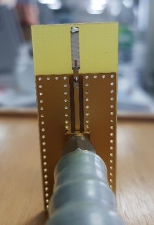
For lower frequency antennas, it is possible to use a 0 Ω resistor to short the pi network to see how the antenna is performing without a matching network. However, at higher frequencies, the parasitic inductance of a 0 Ω resistor becomes significant enough to effect the network. Therefore, a capacitor with its self-resonant frequency at the antenna frequency can be used as a short. In theory, when the capacitor is used at its SRF, the impedance should be resistive and not reactive. Although the capacitor has ohmic impedance, at these frequencies it will work as a short with no reactive element, which is better than a resistor with parasitic reactance. For our example, a 15 pF high-Q RF capacitor was used (Figure 10).
6 Summary
The WE-MCA Multiplayer Chip Antenna can be used for a variety of wireless data applications including Bluetooth, GSM, ZigBee and WLAN. It has a low profile and weight while having high gain and temperature stability. The chip antennas can be easily implemented without specialist knowledge or RF expertise while maintaining performance. The matching of WE-MCA Multilayer Chip Antennas can be a simple process when the fundamentals of impedance measurement and matching are understood and a logical iterative process followed.


.jpg)


.jpg)


.png)


.png)


.png)


.jpg)


.jpg)
.png)


